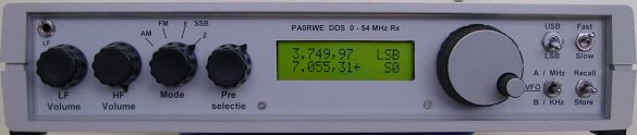
Downloads: Block diagram Digital diagram Front Panel Layout
Because of all my PIC experiences, I started to think about designing a HF receiver controlled by a PIC. After a couple of years with experimenting, building, rebuilding, programming etc. etc. the receiver was ready and worked very well. I will describe the different parts more or less in detail.

Inside view of the RF Receiver
The receiver front-end
On the upper left side of the photograph you see the 4 band filters (0-1.7, 1.7-12, 12-34, 34-54 MHz) designed by PA0RDT. The band filters are switched by relays which are controlled by means of an I2C IC (PCF8574), depending on the chosen reception frequency. Tuning of the filters happens entirely automatic and is based on slowly sweeping an offset voltage on the varicaps. When the signal strength reaches maximum, the process is stopped. The signal strength indication and control of the varicaps’ voltage occur with respectively I2C A/D and D/A converters (TDA8444 and PCF8591). The offset voltage is manually set by the tuning knob, enabled by a certain switch combination, and when it is defined, stored in EEprom.The first IF
On the top left side of the photograph. I used the ‘Frontend‘ pcb of ‘Kent Electronics’ and changed the IF frequency from 45 MHz to 58.1125 MHz because I had the required x-tals available. The N6RY amplifier present on the print has not been used for the LO but to get some extra gain behind the band filters. The unit was built in a metal case.The first oscillator (DDS)
On the top right side of the photograph. The 1st oscillator is a copy of the DDS VFO design of PA0KSB. The only modification I have made is to use a large number of varicaps to reduce the phase noise and to get the needed larger tuning range (58-112 MHz). Also an extra divider was necessary because the VCO frequency was to high for the HCT4040. I used an U664B, to divide the VCO frequency by 64, before it enters the HCT4040. That meant automatically changing of the dividend of the HCT4040 and of course in the software to 2048 in stead of 512. Because of that change, the step size of the tuning knob changed to c.a. 1.2 Hz, what, in my opinion, is still very acceptable. The DDS and VCO are accommodated in the casing of an old TV-tuner.The rotary encoder
See the photograph, directly behind the front plate . The tuning knob firstly was a Bourns encoder with 24 ppo, of which the click mechanism had been removed. This encoder however, was mechanical not exactly great, as a result of which tuning happened sometimes spontaneous automatically! Later on I used an encoder made of the calibration part of a stepper motor used in an IBM plotter. After some mechanical changes it had acceptable dimensions. The number of pulses per rotation from this optical encoder is 360.The second IF, AGC and LF
On the lower left side of the photograph. This is also a design and pcb of ‘Kent Electronics’ with 455 KHz filters of 2, 6 and 12 KHz band width on it. I had some trouble with unwanted HF in the IF part, so I shielded it as you can see on the left. Also considerably attention has been given on decoupling of the power supply lines. Furthermore, the switching between AM and SSB (and in the future FM) is done by means of relays, and that particular receiving mode is also displayed.The PIC and I2C control
On the right side of the photograph. This, for me, is the most beautiful part of the Rx (I like the challenge of programming a PIC with a lot of functionality…).
The PIC takes the whole control of the Rx namely:
· control band filter relays
· fine tuning the band filters (semi automatic)
· measuring the signal strength
· control the DDS
· processing the signals from the tuning knob
· possibility of fast tuning (steps in KHz or MHz)
· memory storage of the VFO frequencies and other receiver parameters for fast start up with the last settings
· memory storage of all 52 band filter tuning offset values (one for each MHz)
· control of the LCDisplay, (with I2C IC PCF8574)The software
Software has been developed by means of the free available development tool MPLAB from Microchip. I used the software fictions of Klaas PA0KSB (SK) to control the DDS and I also used the simplified arithmetic routines. I2C code has also been found on the Internet and has been adapted so that DDS control too could be done via this bus. There are still a couple of program memory bytes left and of the 67 available registers there are still 4 available! Because I did not use interrupts, the consequence was however, that I had to look at the completion of all the control routines very precisely. It is not desirable that, when turning the tuning knob, the display and DDS frequency are not changing directly and at the same moment….!Why I choose for I2C
There are a number of reasons why I have used I2C techniques:
– relatively simply serial protocol (after an 8-bits address always the data follows (read or write)
– the I2C bus consists of two wires only, clock (SCL) and data (SDA)
– the number of I/O ports on the PIC are not sufficient for all functions
– less chance for interfering signals (it is for that reason they are applied in radios and TV’s)
– control of the DDS over the same bus, the DDS, however, demands still 1 line extra on behalf of the internal register targeting (Fsync)
– unique address for each I2C IC as a result of which no conflict exits by controlling the DDS and the several other I2C IC’s